There are two PCBs available using TLE956x motor control ICs.
BLDC Motor Shield with TLE9563
Pinout Diagram
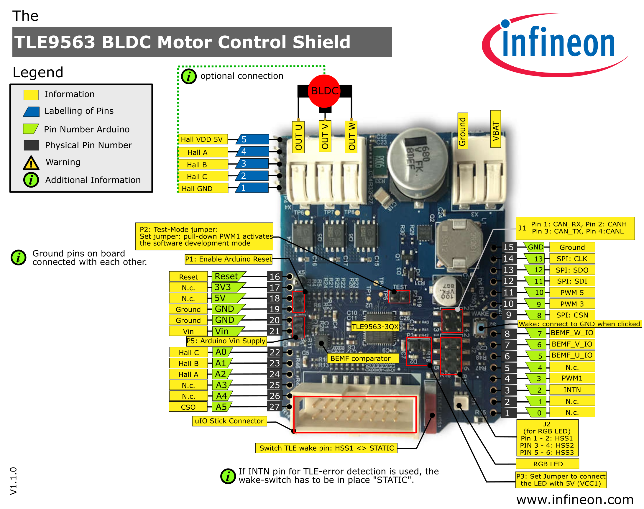
Pin Description
Arduino Pin |
Symbol |
Type |
Function |
|---|---|---|---|
GND |
GND |
- |
Ground |
D2 |
INTN |
Output/digital |
Interrupt output of TLE956x configurable via SPI. |
D3 |
PWM1 |
Input/PWM |
Input PWM for Phase 1 |
D5 |
BEMF_U_IO |
Output/digital |
Output of BEMF comparator for Phase 1 |
D6 |
BEMF_V_IO |
Output/digital |
Output of BEMF comparator for Phase 2 |
D7 |
BEMF_W_IO |
Output/digital |
Output of BEMF comparator for Phase 3 |
D8 |
SPI CSN |
Input/digital |
Chip select pin for SPI communication |
D9 |
PWM 3 |
Input/PWM |
Input PWM for Phase 2 |
D10 |
PWM5 |
Input/PWM |
Input PWM for Phase 3 |
D11 |
SPI SDI |
Input/digital |
Serial Data Input from Microcontroller to TLE |
D12 |
SPI SDO |
Output/digital |
Serial Data Output from TLE to Microcontroller |
D13 |
SPI CLK |
Input/digital |
SPI Clock |
A0 |
Hall C |
Output/digital |
Signal of Hallsensor C (from BLDC motor) |
A1 |
Hall B |
Output/digital |
Signal of Hallsensor B (from BLDC motor) |
A2 |
Hall A |
Output/digital |
Signal of Hallsensor A (from BLDC motor) |
A5 |
CSO |
Output/analog |
Output of current sense amplifier |
Jumper settings
For plug & play operation with the provided example code, it’s recommended to set the default jumpers:
Jumper |
Default |
Function |
|---|---|---|
J1 |
None (only in-/output) |
In and output of the high speed CAN transceiver |
J2 |
set 3 Jumpers |
Connect each High-Side-Switch of the TLE9563 with a color of the RGB LED |
P1 |
set |
Connect RESET of Arduino with RSTN of TLE5963 |
P2 |
set |
Connect the INTN pin of TLE9563 with a pulldown to GND. This enables software development mode. |
P3 |
set |
Connect green LED with VCC1 of TLE9563 indicating chip is powered on |
P4 |
None (only input) |
Connector for hall-sensor |
P5 |
set |
Connect VIN of Arduino with 5V regulator on TLE9563 shield |
For more information refer to the BLDC motor shield user manual and TLE9563-3QX Datasheet.
DC Motor Shield with TLE9562
Pinout Diagram
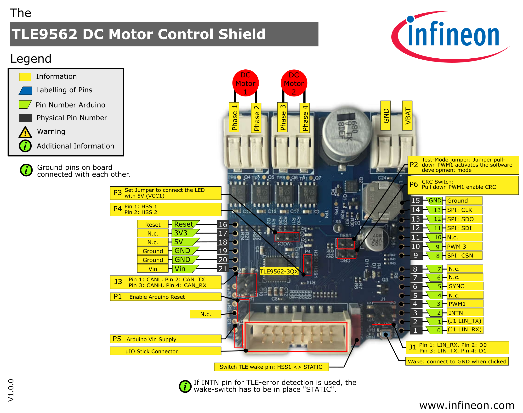
Pin Description
Arduino Pin |
Symbol |
Type |
Function |
|---|---|---|---|
GND |
GND |
- |
Ground |
D2 |
INTN |
Output/digital |
Interrupt output of TLE956x configurable via SPI. |
D3 |
PWM1 |
Input/PWM |
Input PWM for Phase 1 |
D5 |
SYNC |
Input/digital |
Synchronization for wake input |
D8 |
SPI CSN |
Input/digital |
Chip select pin for SPI communication |
D9 |
PWM 3 |
Input/PWM |
Input PWM for Phase 2 |
D11 |
SPI SDI |
Input/digital |
Serial Data Input from Microcontroller to TLE |
D12 |
SPI SDO |
Output/digital |
Serial Data Output from TLE to Microcontroller |
D13 |
SPI CLK |
Input/digital |
SPI Clock |
Jumper Settings
For plug & play operation with the provided example code, it’s recommended to set the default jumpers:
Jumper |
Default |
Function |
|---|---|---|
J1 |
None |
Connect D0 and D1 with LIN transceiver |
J3 |
None (only in-/output) |
In and output of the high speed CAN transceiver |
P1 |
set |
Connect RESET of Arduino with RSTN of TLE5962 |
P2 |
set |
Connect the INTN pin of TLE9562 with a pulldown to GND. This enables software development mode. |
P3 |
set |
Connect green LED with VCC1 of TLE9562 indicating chip is powered on |
P4 |
None (only output) |
Output of remaining High-Side-Switches HSS1 and HSS2. |
P5 |
set |
Connect VIN of Arduino with 5V regulator on TLE9562 shield |
P6 |
None |
Connect the PWM1 pin of TLE9562 with a pulldown to GND. This enables CRC. |
For more information refer to the DC motor shield user manual and TLE9562-3QX Datasheet.